MFM
Protokoll,
Overview
The
MFM
(
Modified
Frequency
Modulation
) procedure was introduced within the patent number 4,376,958
. More details concerning the MFM
can be obtained from several sites in the Internet . The
MFM procedure was used predominantly at hard disks and diskette
drives with the ST506 interface.
DEC
RL02 MFM
DECODER
The
transfer rate at the RL02 disk drives is based on 4.1 magabits/sec
and therefore very difficultly to clone it with the 50 MHz FPGA
Clock . ( 5.0
MHz would be essential and therefore easy to realize at the ST506
interface ).
But there are approaches to solution which I want to introduce in
following 3 chapters.
A) Analysis of the MFM signals and MFM DECODERS without CLOCK RECOVERY
B) Realization of a MFM DECODER with CLOCK and DATA RECOVERY (CDR) by measure the MFM signals.
C) Ready for use MFM DECODER with CLOCK and DATA RECOVERY for DEC RL02 disk drives based on SHIFT REGISTER technology with Clock-Sync.
Remark:
The
RL02 cartridges were factory formated and the Servo/Header format
was strictly company confidential to force purchasing the
expensive, original DEC cartridges only. In the Servo/Header
section of the RL02 disk cartridge format appears sometimes a
0.125uS or 0.625uS MFM signal ( 0.250uS, 0.325uS, 0.500uS is
normal ) which will confuse my MFM decoders, described in chapter
B)
and
C)
Original,
the Servo/Header decoding was realized with a ROM on the RLV-11
controller. To eliminate this undocumented feature in the design
chapter C) , the Servo/header part will be skipped and a re-sync
with byte alignment in the Data preample (PR2) phase which
contains 47 "0" following by a marker "1"
(Sync Bit) is my way to bypass it at this point in time. Unless
the structure of the Servo/Header information ist not 100% clear,
the MFM clock will be disabled for 250uS. Understanding
the Servo/Header structure will become very important by designing
the MFM Encoder and is an ongoing issue for me. From
the present view it would have been much simpler to develop a disk
simulator based on the ST506 interface .
A)
Analysis
of the MFM signals and MFM DECODERS without CLOCK RECOVERY
To
be able to analyse the MFM signals, a test-pattern which always
provides the same contents per sector and track was necessary. I
did generate this required test-pattern with a RT-11
Basic program .
This
was the ideal starting point for an exactly analysis of the MFM
signals. The MFM-data
got
visible on a logic-analyser very well.
The
necessary MFM-decoder for this task was relatively easy to develop
because the required synchronous 4.1 Mhz MFM-clock is available
during a write cycle and is distributed from the RLV-12
controller. The circuit-diagram
looks
correspondingly simple.
At this point, we are already able to decode MFM data, but this method only works if a synchronous clock signal within the MFM signals is available. The second disadvantage of this methode: I have to rebuilt manually all the timing-track/servo/header infos including CRC during the MFM-encoding cycle. Therefore we need a MFM decoder with CLOCK and DATA RECOVERY ( CDR ) to collect all the timing infos from the surface.
B)
Realisierung eines MFM DECODER mit CLOCK
and DATA RECOVERY
(
CDR ), Messen der MFM Signale.
To
reconstruct the clock signal from the MFM data, a PLL is needed
which was typically included on the RLV-11/12 disk controllers.
There
is no PLL in the FPGA world based on the classical form with VCO,
though. Instead of the PLL , the DPLL
algorithm
is used to reconstruct the clock signal from the MFM data.
This
looks as follows at the RL02 disk drive:
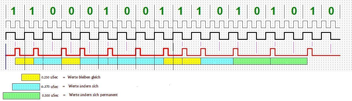
The MFM data are
changed with phase schifting. Different timing periods will arise
into dependency MFM data changed. At the example of the RL02 disk
drive running with a 4.1Mhz
clock will
result in 3 different timing periods which than can be dissolved
as follows are the results:
1)
Short
Period ,
0.250 uS ====>
Value remains the same 1111.... or 0000....
2) Long
Period ,
0.375 uS ====>
Value changes 000111 or 100100
3) Very
long Period, 0.500uS
====> Value changes
continuously 0101010101
Example:
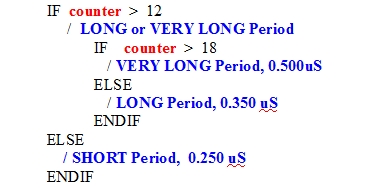
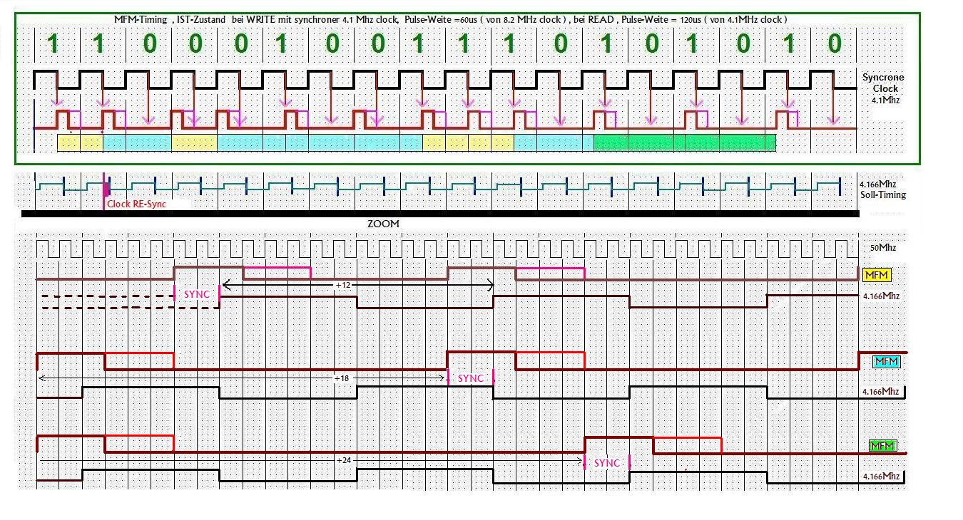
To generate an output signal whose phase is related to the phase of the MFM signal, a considerably higher frequency is necessary to be able to measure the time periods between the MFM signal edges. In the example here with a standard 50Mhz FPGA clock. The 3 different MFM signal periods produce a counter resolution for 12 = short period, 18 = long period and 24 very long period.
The solution for measuring the MFM periods looks that way:
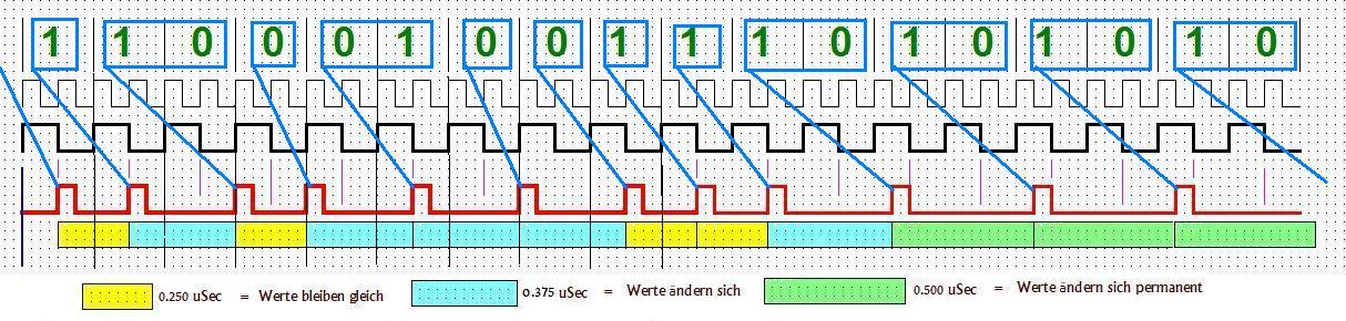
Now, the data still must be produced from the sequence of the different periods. It is important to know that the measuring of the data is always going on around one period afterwards. The algorithm for the MFM decoder looks that way:
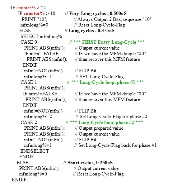
The run down will produce following result:
At the first moment, the algorithm seems to be a little unclear. It lies well, that no clock is provided for the first “0“ if a double “00“ sequenze occurs within the MFM method, so it virtually falls away which saves disk space. Furthermore is valid, that a long MFM period always result in a Bit change. There also is a particularly interesting constellation at a bit sequence “100100100100...“ which has a Long cycle loop the consequence.
Implementation: I
have developed the complete MFM-Decoder
Program in
GFA-Basic/Pascal because nothing quicker gives development and
testing of an algorithm for me.
Status:
This
effective and elegant solution is not completed yet. I want to
implement the algorithm with Verilog
and
to do this, at present, I still have too little experience. If it
is done, I will publish the code. At present, I am able to collect
the MFM cycles via a counter running with the 50Mhz FPGA clock,
send the data to the ARM or NIOSII CPU and decode it. Also here, I
still run in the problem already described in the servo/header
area of the MFM data (see note in overview).
C) Ready for use MFM DECODER with CLOCK and DATA RECOVERY for DEC RL02 disk drives based on SHIFT REGISTER technology with Clock-Sync.
This operational MFM decoder is based on another approach to solution. Unfortunately, it is not possible to reconstruct with the 50Mhz FPGA clock the necessary phase-synchronous 4.1Mhz clock. However, an approximate frequency of 4.1666 Mhz can be obtained using a 12:1 divider using the 50 Mhz standard FPGA clock as input signal. The realization was not simple, though. The following picture illustrates the difficulties:
In dependency of the 3 possible MFM cycles and the current Bit status, the 12:1 divider always has to be synchronized via CLEAR or PRESET to prevent running out of scope. My design is based on a circuit, consisting of the MFM decoder and a serial to 16 bit converter to be able to process the date further into a FIFO, dual port RAM or ARM CPU comfortably. It is possible to read one sector/track with th following components:
Version
1.0
-
Basic
circuit
to
be able to read one sector and/or track.
- Core circuit, the
MFM-DECODER
-
A Serial-16Bit
converter
und
and following supplement components:
- 12:1
Divider
-
Zyklus-Starter
-
2 different 8-16-128 Bit Counters, Typ_A
and
Typ_B
-
Delay
logic
Version
2.0
Up
to now it was not possible to read out the HEADER data from the
disk servo area. Since it is very important to get the the exact
HEADER information for project completion. I have changed
accordingly the MFM-Decoder. The following picture illustrates the
functionality:
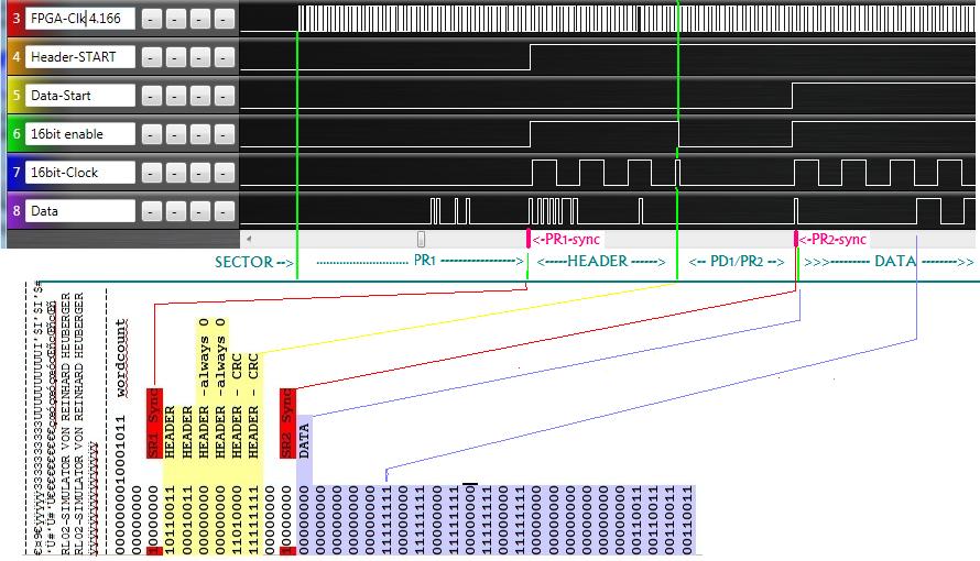
Further upgrade infos can be obtained from the Vintage-Computer-Forum. The new revision edition from my MFM-Decoder Version 2.0 is equipped with a serial and a 16Bit parallel output and the necessary strobe signals. With the following components it is possible to read the HEADER and DATA from one RL02 sector/track:
-
Basic
circuit
to
be able to read one sector and/or track.
- Core circuit, the
MFM-DECODER-V2
Following
supplement components:
- 12:1
Divider
-
Zyklus-Starter
-
16Bit_synchron_counter
-
8_16_64_128_Counter_C
-
Delay
logic
All files are available in JPG format. For Altera/Quartus user, I can provide the entire folder, including programes for the ARM CPU in the ZIP format. If required , please send me an e-mail.