|
Action |
Timeframe |
Status |
|
Install , repair and recover Micro-PDP-11 + RL02 disk drive. |
SEP-2009 |
DONE |
|
Hardware engineering of the RL02 Receive/Transmit Bus-Board based on TTL-logic. --> 1.2 |
SEP/OKT-2009 |
DONE >> Able to monitor/watch the RL02-Bus signals via scope. |
|
Test with PIC MCU's --> 1.3-A) |
OKT-2009 |
DONE, = not useable. |
|
Implementation of ARM-7 MCU based on LPC2148 development board. --> 1.3-B) |
OKT-2009 |
DONE |
|
Development of the Software environment. --> 1.4 |
OKT-2009 - JAN-2010 |
DONE |
|
Hardware engineering, prototype = TTL based logic board to be able to receive and read the RL02 Command Register. Writing C-code for ARM-7 MCU. --> 1.3-C) |
NOV-2009 to JAN-2009 |
DONE
|
|
Installing and customizing MAXII FPGA Hardware + Software + I/O Tests to be able to verify data flow RL02-FPGA-ARM-7 --> 1.3-D) |
DEZ-2009 to JAN-2009 |
DONE
|
|
Design FPGA schematic circuit diagram and write C-Code to be able to receive RL02 Command-Register and send Status-Word. |
FEB-2010 to APR-2010 |
DONE |
|
Install and setup RT-11 environment to be able to write FORTRAN, BASIC or MACRO-11 assembler programs. |
APR-2010 to MAI-2010 |
DONE |
|
Implement Sector-Puls generator running in FPGA |
APR-2010 |
DONE |
|
New investment necessary : Logic Analyser. |
MAI-2010 |
DONE |
|
Implement MFM Decoder running in FPGA. ( 1 of 2 major problem ) |
MAR-2010 to MAI- 2010 |
DONE |
|
Implement MFM Encoder running in FPGA. ( 2 of 2 major problem ) |
MAI-2010 |
Ongoing (most = done ) |
|
Write C-code for the ARM-7 MCU to get access to the SD-card. Fake the RL02 data structures concerning sector size/header and CRC checking. |
FEB-2010 |
Ongoing |
|
Up-to-date
status , 27-MAI-10 : |
|
Implement data transfer, either per Sector oder per Track Financial problem: Investment of new Hardware!
|
?? ?? ?? |
Testing started
I would need a sponsor
|
|
During the summertime of 2010: My last attempt based on the MAXII and ARM-7 environment: The idea was to read one or two ( HEAD-0 and HEAD-1 ) complete tracks into the memory of the ARM-7 MCU. One track contains 40 sectors and one sector contains 280 Bytes, = 11200 Bytes per track x 2 = 22400 Byte ( HEAD-0 and HEAD-1 ). The available Memory on my used ARM-7, LPC2148 is 42K Bytes RAM and this would be enough to hold 2 tracks in the ARM-7 memory. Next step would be to save all tracks on a SD-Card which results in a RL02-like formated SD-Card. This would be an ideal starting point for a much simpler implementation because we have not to take care about Header+CRC sector structures. Sorry, but I was not able to solve this challenge with the current used environment. More details can be gathered from chapter 1.6 and any input/hints to this issue is very welcome. |
|
Up-to-date status, 20-AUG-10: I
made another investment with the following
product: |
|
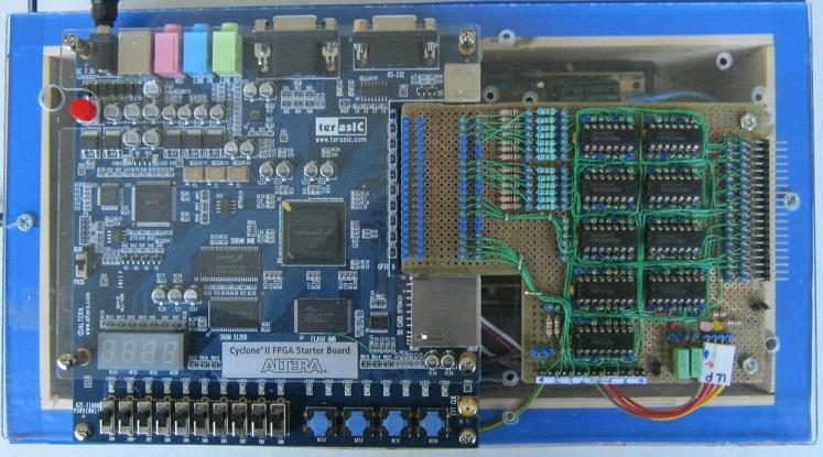
The following picture shows the new DE1 board based on Cyclone® II from Altera. To be able to connect the RL02 bus-signals to the DE1 board an new adapter board must also be developed and is visible in the right part. |
|
|
|
Implement new environment and replace ARM C-Code by NIOS
C-Code. |
SEP-2010
OCT-2010 |
EXIT |
|
|
|
I could solve the problem as described above by replacing the DC005 and the DC004 Q-Bus chips. Unfortunately, an error has happened to me when soldering and now I have contact problems. The RLV-12 controller does not always work and sometimes I have to replug it several times until I can continue to work. This handicaps me in my work very much and I am continuous searching for a replacement. Again, any help is welcome |
|
The project goes on. A MFM decoder with Clock and Data Recovery ( CDR ) is available and up and running. For more details, see chapter 1.7 |
|
Fix and implement all open issues from MAXII environment in the new DE1 board environment. |
FEB-2011 |
Ongoing
|
-
In view of the very sad events in Japan, I can't enjoy continuing to work at the moment!
|
The development based on blockdiagram got more problematic and inefficient. I have given up this kind of development and replaced most of my modules by Verilog programs. |
FEB-2011
JUL-2011 |
Closed
|
|
SD Card I/O implemented to be able to reconstruct the RL02 Format on a SD Card via NIOSII system. |
MAR-2011 JUN-2011 |
Closed
|
|
Developing data/timing sequencer and dual port RAM Verilog design. |
MAY-2011 JUL-2011 |
Closed
|